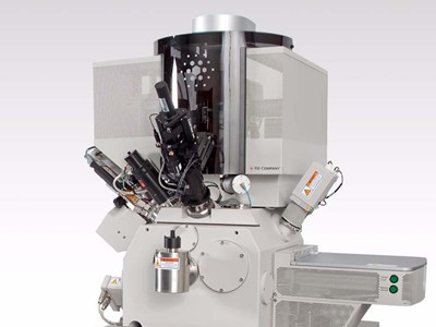
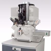

The FEI Helios NanoLab 450 / 450S DualBeam systems integrate ion and electron beams for FIB and SEM functionality in one machine. Users can switch between the two beams for quick and accurate navigation and milling. Convergence of the SEM and FIB at short working distance allows precision “slice-and-view” cross-sectioning and analysis at high resolution. FIB/SEM DualBeam systems provide an expanded range of capabilities not possible with separate FIB and SEM tools:
•Electron beam high-resolution imaging of FIB cross sections without eroding the feature of interest.
•Real-time cross-section electron beam imaging during FIB milling.
•Focused electron beam charge neutralization during FIB milling.
•Focused ion beam charge neutralization during SEM imaging.
•High resolution elemental microanalysis of defect cross sections.
•Sample surface imaging with the electron beam during navigation without erosion or gallium implantation from the ion beam.
•TEM sample preparation with in situ conductive coating. The Tomahawk™ ion column provides fast, precise milling and high-resolution imaging of the sample surface. The Elstar electron column takes advantage of FEI’s most advanced Hexalens™ design for ultimate image resolution at low beam energies. It offers nondestructive imaging capability at a working distance optimized for ultrahigh resolution and can display samples magnified over 500 000× in mode 1 and > 2 500 000× in mode 2. The Helios NanoLab was designed for imaging nanostructures of any material (man-made, biological, natural), particularly in the area of:
•Nanoelectronics,
•Process yield engineering,
•Biology. The system was designed for:
•Data storage
•Process yield engineering
•Etching
•Lithography
•Metal and other materials deposition
•Fabrication of micro- and nanostructures